Si4712/13-B30
4
Rev. 1.1
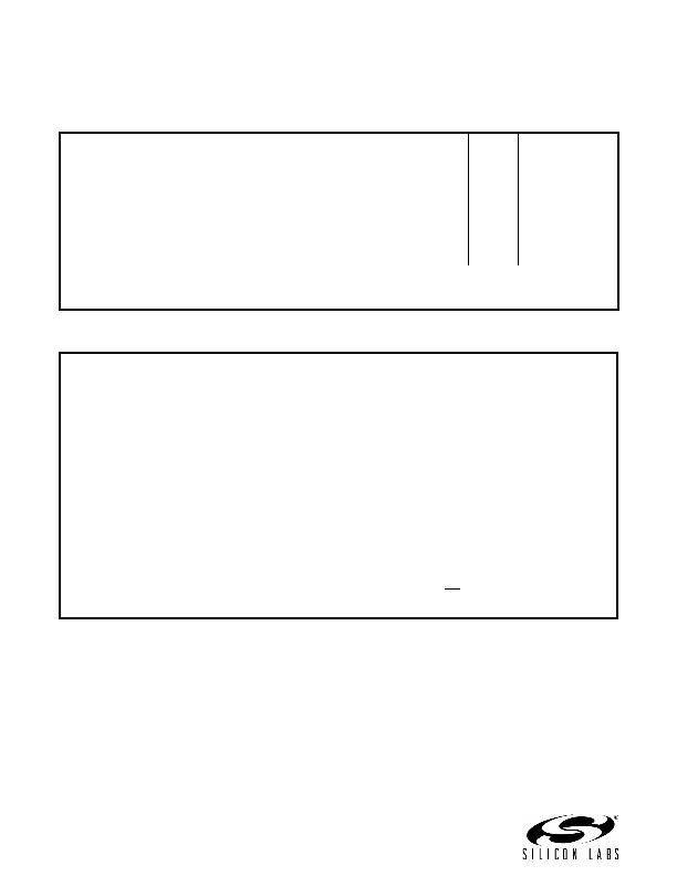
1. Electrical Specifications
Table 1. Recommended Operating Conditions
Parameter
Symbol
Test Condition
Min
Typ
Max
Unit
Supply Voltage
V
DD
2.7
5.5
V
Interface Supply Voltage
V
IO
1.5
3.6
V
Power Supply Powerup Rise Time V
DDRISE
10
祍
Interface Supply Powerup Rise
Time
V
IORISE
10
祍
Ambient Temperature
T
A
20
25
85
癈
Note: All minimum and maximum specifications are guaranteed and apply across the recommended operating conditions.
Typical values apply at V
DD
= 3.3 V and 25 癈 unless otherwise stated. Parameters are tested in production unless
otherwise stated.
Table 2. Absolute Maximum Ratings
1,2
Parameter
Symbol
Value
Unit
Supply Voltage
V
DD
0.5 to 5.8
V
Interface Supply Voltage
V
IO
0.5 to 3.9
V
Input Current
3
I
IN
10
mA
Input Voltage
3
V
IN
0.3 to (V
IO
+ 0.3)
V
Operating Temperature
T
OP
40 to 95
癈
Storage Temperature
T
STG
55 to 150
癈
RF Input Level
4
0.4
V
PK
Notes:
1. Permanent device damage may occur if the absolute maximum ratings are exceeded. Functional operation should be
restricted to the conditions as specified in the operational sections of this data sheet. Exposure beyond recommended
operating conditions for extended periods may affect device reliability.
2. The Si4712/13 devices are high-performance RF integrated circuits with certain pins having an ESD rating of < 2 kV
HBM. Handling and assembly of these devices should only be done at ESD-protected workstations.
3. For input pins SCLK, SEN, SDIO, RST, RCLK, DCLK, DFS, DIN, GPO1, GPO2/INT
, and GPO3.
4. At RF input pin, TXO.
发布紧急采购,3分钟左右您将得到回复。
相关PDF资料
SKY12146-321LF
IC VAR VOLT ATTEN 12QFN
SN171GG-NR
SNAP PROTOBOARD W/NO RADIO
SWLP.2450.12.4.B.02
ANTENNA WI-FI WLAN 2.4GHZ
TD4A
SENSOR RTD LIQUID TEMP 2TERM
TD5A
SENSOR RTD TEMP MINI 3LEAD
TG.09.0113W
ANT 5-BAND GSM HINGE TERMINAL
TG.09.0113
ANT 5-BAND GSM HINGE TERMINAL
TG.10.0113
RF ANTENNA
相关代理商/技术参数
SI4713-B-EVB
功能描述:射频开发工具 SI4713 EVAL BOARD REV B RoHS:否 制造商:Taiyo Yuden 产品:Wireless Modules 类型:Wireless Audio 工具用于评估:WYSAAVDX7 频率: 工作电源电压:3.4 V to 5.5 V
SI4714DY
制造商:VISHAY 制造商全称:Vishay Siliconix 功能描述:N-Channel 30 V (D-S) MOSFET with Schottky Diode
Si4714DY-T1-GE3
功能描述:MOSFET 30 Volts 13.6 Amps 4.5 Watts
RoHS:否 制造商:STMicroelectronics 晶体管极性:N-Channel 汲极/源极击穿电压:650 V 闸/源击穿电压:25 V 漏极连续电流:130 A 电阻汲极/源极 RDS(导通):0.014 Ohms 配置:Single 最大工作温度: 安装风格:Through Hole 封装 / 箱体:Max247 封装:Tube
SI4719CY
功能描述:电源开关 IC - 配电 P-Ch Battery Switch RoHS:否 制造商:Exar 输出端数量:1 开启电阻(最大值):85 mOhms 开启时间(最大值):400 us 关闭时间(最大值):20 us 工作电源电压:3.2 V to 6.5 V 电源电流(最大值): 最大工作温度:+ 85 C 安装风格:SMD/SMT 封装 / 箱体:SOT-23-5
SI4719CY-E3
功能描述:电源开关 IC - 配电 P-Ch Battery Switch RoHS:否 制造商:Exar 输出端数量:1 开启电阻(最大值):85 mOhms 开启时间(最大值):400 us 关闭时间(最大值):20 us 工作电源电压:3.2 V to 6.5 V 电源电流(最大值): 最大工作温度:+ 85 C 安装风格:SMD/SMT 封装 / 箱体:SOT-23-5
SI4719CY-T1-E3
功能描述:电源开关 IC - 配电 P-Ch Battery Switch RoHS:否 制造商:Exar 输出端数量:1 开启电阻(最大值):85 mOhms 开启时间(最大值):400 us 关闭时间(最大值):20 us 工作电源电压:3.2 V to 6.5 V 电源电流(最大值): 最大工作温度:+ 85 C 安装风格:SMD/SMT 封装 / 箱体:SOT-23-5
SI4720
制造商:SILABS 制造商全称:SILABS 功能描述:Broadcast FM Radio Transceiver for Portable Applications
Si4720-A10-GM
功能描述:射频收发器 Broadcast FM Radio Transceiver RoHS:否 制造商:Atmel 频率范围:2322 MHz to 2527 MHz 最大数据速率:2000 Kbps 调制格式:OQPSK 输出功率:4 dBm 类型: 工作电源电压:1.8 V to 3.6 V 最大工作温度:+ 85 C 接口类型:SPI 封装 / 箱体:QFN-32 封装:Tray